|
|
• 16-channel DAC in 52-lead LQFP and 56-lead LFCSP
packages
|
• Guaranteed monotonic to 16/14 bits
|
• Nominal output voltage range of −10 V to +10 V
|
• Multiple output spans available
|
• Temperature monitoring function
|
• Channel monitoring multiplexer
|
• GPIO function
|
• System calibration function allowing user-programmable
offset and gain
|
• Channel grouping and addressing features
|
• Data error checking feature
|
• SPI-compatible serial interface
|
• 2.5 V to 5.5 V digital interface
|
|
| CATALOG |
| AD5360BSTZ COUNTRY OF ORIGIN |
AD5360BSTZ PARAMETRIC INFO
|
AD5360BSTZ PACKAGE INFO
|
AD5360BSTZ MANUFACTURING INFO
|
AD5360BSTZ PACKAGING INFO
|
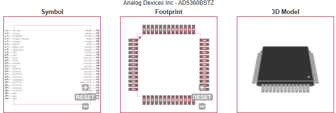
AD5360BSTZ ECAD MODELS
|
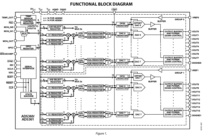
AD5360BSTZ FUNCTIONAL BLOCK DIAGRAM
|
AD5360BSTZ APPLICATIONS
|
|
COUNTRY OF ORIGIN
|
| China |
Ireland
|
Philippines
|
|
PARAMETRIC INFO
|
| Architecture |
Resistor-String |
| Resolution |
16bit |
| Number of DAC Channels |
16 |
| Number of Outputs per Chip |
16 |
| Converter Type |
General Purpose |
| Output Type |
Voltage |
| Voltage Reference |
External |
| Maximum Settling Time (us) |
30 |
| Digital Interface Type |
Serial (4-Wire, SPI, QSPI, Microwire) |
| Output Polarity |
Bipolar |
| Integral Nonlinearity Error |
±4LSB |
| Full Scale Error |
±20mV |
| Minimum Operating Temperature (°C) |
-40 |
| Maximum Operating Temperature (°C) |
85 |
| Supplier Temperature Grade |
Industrial |
| Power Supply Type |
Dual |
| Minimum Dual Supply Voltage (V) |
-4.5/8 |
| Typical Dual Supply Voltage (V) |
±9/-5|±12/-5|±15/-5 |
| Maximum Dual Supply Voltage (V) |
±16.5 |
| Digital Supply Support |
Yes |
| Maximum Power Dissipation (mW) |
245 |
|
|
PACKAGE INFO
|
| Supplier Package |
LQFP |
| Basic Package Type |
Lead-Frame SMT |
| Pin Count |
52 |
| Lead Shape |
Gull-wing |
| PCB |
52 |
| Tab |
N/R |
| Pin Pitch (mm) |
0.65 |
| Package Length (mm) |
10 |
| Package Width (mm) |
10 |
| Package Height (mm) |
1.4 |
| Package Diameter (mm) |
N/R |
| Seated Plane Height (mm) |
1.6(Max) |
| Mounting |
Surface Mount |
| Package Material |
Plastic |
| Package Description |
Low Profile Quad Flat Package |
| Package Family Name |
QFP |
| Jedec |
MS-026BCC |
| Package Outline |
Link to Datasheet |
|
|
MANUFACTURING INFO
|
| MSL |
3 |
| Maximum Reflow Temperature (°C) |
260 |
| Reflow Solder Time (Sec) |
30 |
| Number of Reflow Cycle |
3 |
| Standard |
J-STD-020D |
| Maximum Wave Temperature (°C) |
N/R |
| Wave Solder Time (Sec) |
N/R |
| Lead Finish(Plating) |
Matte Sn annealed |
| Under Plating Material |
Ag |
| Terminal Base Material |
Cu Alloy |
|
|
PACKAGING INFO
|
| Packaging |
Tray |
| Quantity Of Packaging |
160 |
| Packaging Document |
Link to Datasheet |
|
|
ECAD MODELS
|
|
|
FUNCTIONAL BLOCK DIAGRAM
|
|
|
APPLICATIONS
|
• Instrumentation
|
• Industrial control systems
|
• Level setting in automatic test equipment (ATE)
|
• Variable optical attenuators (VOA)
|
• Optical line cards
|
| |