|
|
• Low power: 368 µA maximum quiescent current
|
• Rail-to-rail output
|
• Low noise and distortion
|
• Excellent ac specifications
|
• High precision dc performance (AD8422BRZ)
|
• Wide supply range
|
• Input overvoltage protection: 40 V from opposite supply
|
• Gain range: 1 to 1000
|
• Available in 8-lead LFCSP, 8-lead MSOP, and 8-lead SOIC_N
|
|
| CATALOG |
| AD8422BRMZ-R7 COUNTRY OF ORIGIN |
AD8422BRMZ-R7 PARAMETRIC INFO
|
AD8422BRMZ-R7 PACKAGE INFO
|
AD8422BRMZ-R7 MANUFACTURING INFO
|
AD8422BRMZ-R7 PACKAGING INFO
|
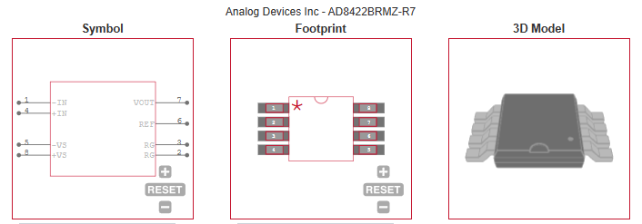
AD8422BRMZ-R7 ECAD MODELS
|
AD8422BRMZ-R7 FUNCTIONAL BLOCK DIAGRAM
|
AD8422BRMZ-R7 APPLICATIONS
|
|
COUNTRY OF ORIGIN
|
China
|
Ireland
|
|
PARAMETRIC INFO
|
| Rail to Rail |
Rail to Rail Output |
| Number of Channels per Chip |
1 |
| Maximum Input Offset Voltage (mV) |
0.05@±15V |
| Maximum Input Bias Current (uA) |
0.0005@±15V |
| Minimum CMRR (dB) |
80 |
| Maximum Quiescent Current (mA) |
0.368@±15V |
| Minimum CMRR Range (dB) |
75 to 85 |
| Minimum Single Supply Voltage (V) |
4.6 |
| Maximum Single Supply Voltage (V) |
36 |
| Minimum Dual Supply Voltage (V) |
±2.3 |
| Maximum Input Resistance (MOhm) |
200000(Typ)@±15V |
| Maximum Dual Supply Voltage (V) |
±18 |
| Maximum Voltage Gain Range (dB) |
60 to 75 |
| Maximum Voltage Gain (dB) |
60 |
| Minimum Operating Temperature (°C) |
-40 |
| Maximum Operating Temperature (°C) |
85 |
| Minimum Storage Temperature (°C) |
-65 |
| Maximum Storage Temperature (°C) |
150 |
| Power Supply Type |
Single|Dual |
| Maximum Supply Voltage Range (V) |
30 to 50 |
| Typical Single Supply Voltage (V) |
5|9|12|15|18|24|28 |
| Typical Dual Supply Voltage (V) |
±3|±5|±9|±12|±15 |
| Maximum Operating Supply Voltage (V) |
±18|36 |
|
|
PACKAGE INFO
|
| Supplier Package |
MSOP |
| Basic Package Type |
Lead-Frame SMT |
| Pin Count |
8 |
| Lead Shape |
Gull-wing |
| PCB |
8 |
| Tab |
N/R |
| Pin Pitch (mm) |
0.65 |
| Package Length (mm) |
3 |
| Package Width (mm) |
3 |
| Package Height (mm) |
0.85 |
| Package Diameter (mm) |
N/R |
| Package Overall Length (mm) |
3 |
| Package Overall Width (mm) |
4.9 |
| Package Overall Height (mm) |
1.1(Max) |
| Seated Plane Height (mm) |
1.1(Max) |
| Mounting |
Surface Mount |
| Package Weight (g) |
N/A |
| Package Material |
Plastic |
| Package Description |
Micro Small Outline Package |
| Package Family Name |
SOP |
| Jedec |
MO-187AA |
| Package Outline |
Link to Datasheet |
|
|
MANUFACTURING INFO
|
| MSL |
1 |
| Maximum Reflow Temperature (°C) |
260 |
| Reflow Solder Time (Sec) |
30 |
| Number of Reflow Cycle |
3 |
| Standard |
J-STD-020D |
| Maximum Wave Temperature (°C) |
N/R |
| Wave Solder Time (Sec) |
N/R |
| Lead Finish(Plating) |
Matte Sn annealed |
| Under Plating Material |
Ag |
| Terminal Base Material |
Cu Alloy |
|
|
PACKAGING INFO
|
| Packaging Suffix |
R7 |
| Packaging |
Tape and Reel |
| Quantity Of Packaging |
1000 |
| Reel Diameter (in) |
7 |
| Packaging Document |
Link to Datasheet |
|
|
ECAD MODELS
|
|
|
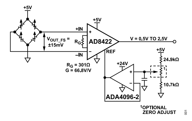
TYPICAL APPLICATION DIAGRAM
|
|
|
APPLICATIONS
|
• Medical instrumentation
|
• Industrial process controls
|
• Strain gages
|
• Precision data acquisition systems
|
• Transducer interfaces
|
• Channel-isolated systems
|
• Portable instrumentation
|
|