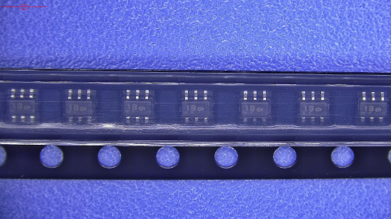
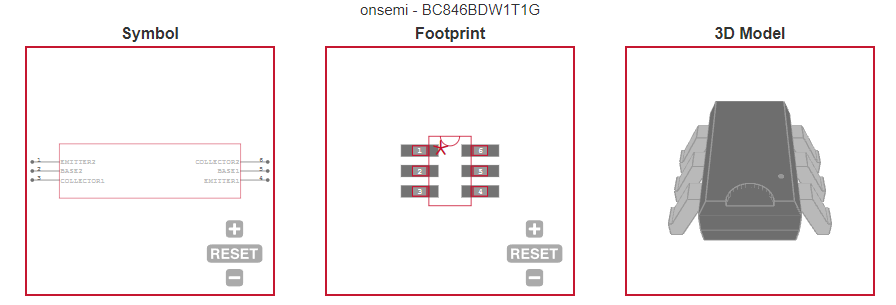
BC846BDW1T1G onsemi TRANS 2NPN 65V 0.1A SOT363

label:
2023/12/7 271


• S and NSV Prefixes for Automotive and Other Applications Requiring Unique Site and Control Change Requirements; AEC−Q101 Qualified and PPAP Capable
• These Devices are Pb−Free, Halogen Free/BFR Free and are RoHS Compliant*


CATALOG
BC846BDW1T1G COUNTRY OF ORIGIN
BC846BDW1T1G PARAMETRIC INFO
BC846BDW1T1G PACKAGE INFO
BC846BDW1T1G MANUFACTURING INFO
BC846BDW1T1G PACKAGING INFO   
BC846BDW1T1G ECAD MODELS


COUNTRY OF ORIGIN
China
Japan
Malaysia
Morocco
United States of America


PARAMETRIC INFO
Type NPN
Configuration Dual
Maximum Collector-Emitter Voltage (V) 65
Maximum Collector Base Voltage (V) 80
Maximum Emitter Base Voltage (V) 6
Maximum DC Collector Current (A) 0.1
Minimum Transition Frequency (MHz) 100
Maximum Power Dissipation (mW) 380
Typical Output Capacitance (pF) 4.5(Max)
Maximum Junction Ambient Thermal Resistance 328°C/W
Maximum Noise Figure (dB) 10
Operating Junction Temperature (°C) -55 to 150
Maximum Collector Cut-Off Current (nA) 15
Maximum Collector-Emitter Saturation Voltage (V) 0.25@0.5mA@10mA|0.6@5mA@100mA
Maximum Base Emitter Saturation Voltage (V) 0.7(Typ)@0.5mA@10mA|0.9(Typ)@5mA@100mA
Category Bipolar Small Signal
Minimum DC Current Gain 200@2mA@5V
Number of Elements per Chip 2
Minimum Storage Temperature (°C) -55
Maximum Storage Temperature (°C) 150
Minimum Operating Temperature (°C) -55
Maximum Operating Temperature (°C) 150
 
PACKAGE INFO
Supplier Package SC-88
Basic Package Type Lead-Frame SMT
Pin Count 6
Lead Shape Gull-wing
PCB 6
Tab N/R
Pin Pitch (mm) 0.65
Package Length (mm) 2
Package Width (mm) 1.25
Package Height (mm) 0.9
Package Diameter (mm) N/R
Package Overall Length (mm) 2
Package Overall Width (mm) 2.1
Package Overall Height (mm) 1.1(Max)
Seated Plane Height (mm) 1.1(Max)
Mounting Surface Mount
Package Weight (g) N/A
Package Material Plastic
Package Description Small Outline Transistor
Package Family Name SOT
Jedec N/A
 
MANUFACTURING INFO
MSL 1
Maximum Reflow Temperature (°C) 260
Reflow Solder Time (Sec) 30
Number of Reflow Cycle 3
Standard N/A
Reflow Temp. Source Link to Datasheet
Maximum Wave Temperature (°C) N/R
Wave Solder Time (Sec) N/R
Lead Finish(Plating) Matte Sn annealed
Under Plating Material N/A
Terminal Base Material FeNi Alloy
Number of Wave Cycles N/R
 
PACKAGING INFO
Packaging Suffix T1
Packaging Tape and Reel
Quantity Of Packaging 3000
Reel Diameter (in) 7
Reel Width (mm) 8.4(Min)
Tape Pitch (mm) 4
Tape Width (mm) 8
Feed Hole Pitch (mm) 4
Hole Center to Component Center (mm) 2
Component Orientation Q2
Packaging Document Link to Datasheet
Tape Type Embossed
 
ECAD MODELS


Продукт RFQ