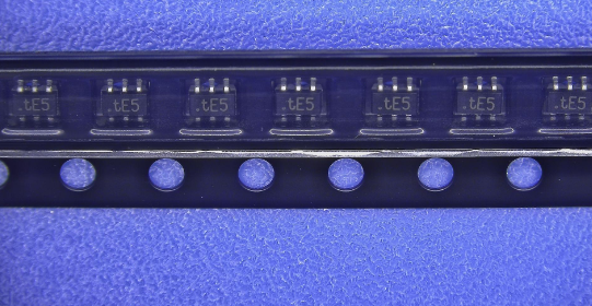
BC846BS Nexperia SOT-363 NPN+NPN 0.3W 0.1A 80V Tr

label:
2025/03/7 68
BC846BS Nexperia SOT-363 NPN+NPN 0.3W 0.1A 80V Tr


• Low collector capacitance
• Low collector-emitter saturation voltage
• Closely matched current gain
• Reduces number of components and board space
• No mutual interference between the transistors


CATALOG
BC846BS COUNTRY OF ORIGIN
BC846BS PARAMETRIC INFO
BC846BS PACKAGE INFO
BC846BS MANUFACTURING INFO
BC846BS PACKAGING INFO
BC846BS APPLICATIONS


COUNTRY OF ORIGIN
China
Malaysia


PARAMETRIC INFO
Type NPN
Configuration Dual
Maximum Collector-Emitter Voltage (V) 65
Maximum Collector Base Voltage (V) 80
Maximum Emitter Base Voltage (V) 6
Maximum DC Collector Current (A) 0.1
Minimum Transition Frequency (MHz) 100
Maximum Power Dissipation (mW) 300
Typical Output Capacitance (pF) 1.9
Maximum Noise Figure (dB) 3.1(Typ)
Operating Junction Temperature (°C) 150
Maximum Emitter Cut-Off Current (nA) 100
Maximum Junction Ambient Thermal Resistance 625°C/W
Typical Input Capacitance (pF) 11
Collector Current for VCE Saturation (mA) 10|100
Maximum Collector Cut-Off Current (nA) 15
Maximum Collector-Emitter Saturation Voltage (V) 0.1@0.5mA@10mA|0.3@5mA@100mA
Maximum Base Emitter Saturation Voltage (V) 0.85@0.5mA@10mA
Category Bipolar Small Signal
Minimum DC Current Gain 200@2mA@5V
Number of Elements per Chip 2
Minimum Storage Temperature (°C) -65
Maximum Storage Temperature (°C) 150
Minimum Operating Temperature (°C) -55
Maximum Operating Temperature (°C) 150


PACKAGE INFO
Supplier Package TSSOP
Pin Count 6
PCB 6
Tab N/R
Package Length (mm) 2.2(Max)
Package Width (mm) 1.35(Max)
Package Height (mm) 1(Max)
Package Diameter (mm) N/R
Mounting Surface Mount
Package Weight (g) N/A
Package Family Name SO
Package Outline Link to Datasheet


MANUFACTURING INFO
MSL 1
Maximum Reflow Temperature (°C) 260
Reflow Solder Time (Sec) 30
Number of Reflow Cycle 3
Standard N/A
Reflow Temp. Source Link to Datasheet
Maximum Wave Temperature (°C) N/R
Wave Solder Time (Sec) N/R
Wave Temp. Source Link to Datasheet
Lead Finish(Plating) Sn
Under Plating Material CuAg
Terminal Base Material FeNi Alloy
Number of Wave Cycles N/R


PACKAGING INFO
Packaging Document Link to Datasheet


APPLICATIONS
• General-purpose switching and amplification

Продукт RFQ