 |
||||||||||||||||||||||||||||||||||||||||||
| |
||||||||||||||||||||||||||||||||||||||||||
| • AEC-Q100 qualified for automotive applications – Device temperature grade 2: –40℃ to +105℃ ambient operating temperature range |
||||||||||||||||||||||||||||||||||||||||||
| • Dual deserializer hub aggregates one or two active sensors over FPD-Link III interface | ||||||||||||||||||||||||||||||||||||||||||
| • Power-Over-Coax (PoC) compatible transceiver | ||||||||||||||||||||||||||||||||||||||||||
| • MIPI DPHY Version 1.2 / CSI-2 Version 1 .3
compliant – CSI-2 output ports – Supports 1, 2, 3, 4 data lanes – CSI-2 data rate scalable for 400 Mbps / 800 Mbps / 1.5 Gbps / 1.6 Gbps each data lane – Programmable data types – Four virtual channels – ECC and CRC generation |
||||||||||||||||||||||||||||||||||||||||||
| • 2x2 Output replication mode | ||||||||||||||||||||||||||||||||||||||||||
| • Ultra-low data and control path latency | ||||||||||||||||||||||||||||||||||||||||||
| • Supports single-ended coaxial or Shielded Twisted-Pair (STP) cable | ||||||||||||||||||||||||||||||||||||||||||
| • Adaptive receive equalization | ||||||||||||||||||||||||||||||||||||||||||
| • I2C with fast-mode plus up to 1 Mbps | ||||||||||||||||||||||||||||||||||||||||||
| • Flexible GPIOs for camera synchronization and diagnostics | ||||||||||||||||||||||||||||||||||||||||||
| • Compatible with DS90UB935-Q1, DS90UB953- Q1, DS90UB933-Q1 and DS90UB913A-Q1 serializers | ||||||||||||||||||||||||||||||||||||||||||
| • Line fault detection and advanced diagnostics | ||||||||||||||||||||||||||||||||||||||||||
| • ISO 10605 and IEC 61000-4-2 ESD compliant | ||||||||||||||||||||||||||||||||||||||||||
| |
||||||||||||||||||||||||||||||||||||||||||
| CATALOG | ||||||||||||||||||||||||||||||||||||||||||
| DS90UB954TRGZRQ1 COUNTRY OF ORIGIN | ||||||||||||||||||||||||||||||||||||||||||
| DS90UB954TRGZRQ1 PARAMETRIC INFO | ||||||||||||||||||||||||||||||||||||||||||
| DS90UB954TRGZRQ1 PACKAGE INFO | ||||||||||||||||||||||||||||||||||||||||||
| DS90UB954TRGZRQ1 MANUFACTURING INFO | ||||||||||||||||||||||||||||||||||||||||||
| DS90UB954TRGZRQ1 PACKAGING INFO | ||||||||||||||||||||||||||||||||||||||||||
| DS90UB954TRGZRQ1 ECAD MODELS | ||||||||||||||||||||||||||||||||||||||||||
| DS90UB954TRGZRQ1 FUNCTIONAL BLOCK DIAGRAM | ||||||||||||||||||||||||||||||||||||||||||
| DS90UB954TRGZRQ1APPLICATIONS | ||||||||||||||||||||||||||||||||||||||||||
| |
||||||||||||||||||||||||||||||||||||||||||
| COUNTRY OF ORIGIN | ||||||||||||||||||||||||||||||||||||||||||
| Philippines | ||||||||||||||||||||||||||||||||||||||||||
| |
||||||||||||||||||||||||||||||||||||||||||
| PARAMETRIC INFO | ||||||||||||||||||||||||||||||||||||||||||
|
||||||||||||||||||||||||||||||||||||||||||
| PACKAGE INFO | ||||||||||||||||||||||||||||||||||||||||||
|
||||||||||||||||||||||||||||||||||||||||||
| MANUFACTURING INFO | ||||||||||||||||||||||||||||||||||||||||||
|
||||||||||||||||||||||||||||||||||||||||||
| PACKAGING INFO | ||||||||||||||||||||||||||||||||||||||||||
|
||||||||||||||||||||||||||||||||||||||||||
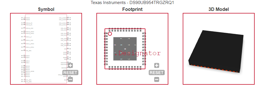
| ECAD MODELS | ||||||||||||||||||||||||||||||||||||||||||
 |
||||||||||||||||||||||||||||||||||||||||||
| |
||||||||||||||||||||||||||||||||||||||||||
| FUNCTIONAL BLOCK DIAGRAM | ||||||||||||||||||||||||||||||||||||||||||
 |
||||||||||||||||||||||||||||||||||||||||||
| |
||||||||||||||||||||||||||||||||||||||||||
| APPLICATIONS | ||||||||||||||||||||||||||||||||||||||||||
| • Automotive ADAS – Rear View Cameras (RVC) – Surround View Systems (SVS) – Camera Monitor Systems (CMS) – Forward Vision Cameras (FC) – Driver Monitoring Systems (DMS) – Satellite RADAR, Time of Flight (ToF) and LIDAR Sensor Modules |
||||||||||||||||||||||||||||||||||||||||||
| • Security and Surveillance | ||||||||||||||||||||||||||||||||||||||||||
| • Industrial and Medical Imaging | ||||||||||||||||||||||||||||||||||||||||||
| |