|
|
• Low Noise Figure: 10 dB
|
• High linearity: In-Band Output IP3 > +30 dBm In-Band Output IP2 > +60 dBm
|
• Pre-programmed and/or Programmable Bandwidth: 5 MHz to 72 MHz. (Please see HMC1023LP5E Ordering Information)
|
• Exceptional 3 dB Bandwidth Accuracy: ±2.5%
|
• Programmable Gain: 0 or 10 dB
|
• Integrated ADC Driver Amplifier
|
• 6th order Butterworth Magnitude & Phase Response
|
• Automatic Filter Calibration
|
• Externally Controlled Common Mode Output Level
|
• Filter Bypass Option
|
• Pin & Register Compatible to HMC900LP5E
|
|
| CATALOG |
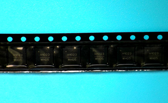
HMC1023LP5E COUNTRY OF ORIGIN
|
| HMC1023LP5E LIFECYCLE |
HMC1023LP5E PARAMETRIC INFO
|
HMC1023LP5E PACKAGE INFO
|
HMC1023LP5E MANUFACTURING INFO
|
HMC1023LP5E PACKAGING INFO
|
HMC1023LP5E ECAD MODELS
|
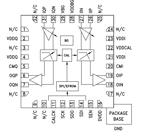
HMC1023LP5E FUNCTIONAL DIAGRAM
|
HMC1023LP5E APPLICATIONS
|
|
COUNTRY OF ORIGIN
|
Malaysia
|
|
| LIFECYCLE |
Obsolete
Aug 31,2022 |
|
PARAMETRIC INFO
|
| Type |
Low Pass Filter |
| Number of Circuits |
2 |
| Cut-Off Frequency Range |
>=6MHz |
| Maximum Order |
6th |
| Cut-Off Frequency |
72MHz(Max) |
| Power Supply Type |
Single |
| Operating Supply Voltage (V) |
5 |
| Minimum Single Supply Voltage (V) |
4.75 |
| Typical Single Supply Voltage (V) |
5 |
| Maximum Single Supply Voltage (V) |
5.25 |
| Minimum Operating Temperature (°C) |
-40 |
| Maximum Operating Temperature (°C) |
85 |
| Minimum Storage Temperature (°C) |
-65 |
| Maximum Storage Temperature (°C) |
150 |
|
|
PACKAGE INFO
|
| Supplier Package |
QFN EP |
| Basic Package Type |
Non-Lead-Frame SMT |
| Pin Count |
32 |
| Lead Shape |
No Lead |
| PCB |
32 |
| Tab |
N/R |
| Pin Pitch (mm) |
0.56(Max) |
| Package Length (mm) |
5.1(Max) |
| Package Width (mm) |
5.1(Max) |
| Package Height (mm) |
0.95(Max) |
| Package Diameter (mm) |
N/R |
| Seated Plane Height (mm) |
1(Max) |
| Mounting |
Surface Mount |
| Package Material |
Plastic |
| Package Description |
Quad Flat No Lead Package, Exposed Pad |
| Package Family Name |
QFN |
| Package Outline |
Link to Datasheet |
|
|
MANUFACTURING INFO
|
| MSL |
1 |
| Maximum Reflow Temperature (°C) |
260 |
| Reflow Solder Time (Sec) |
40 |
| Reflow Temp. Source |
Link to Datasheet |
| Maximum Wave Temperature (°C) |
N/R |
| Wave Solder Time (Sec) |
N/R |
| Wave Temp. Source |
Link to Datasheet |
| Lead Finish(Plating) |
Matte Sn annealed |
| Under Plating Material |
Ag |
| Terminal Base Material |
Cu Alloy |
|
|
PACKAGING INFO
|
| Packaging |
Tape and Reel |
| Quantity Of Packaging |
500 |
|
|
| ECAD MODELS |
 |
|
| FUNCTIONAL DIAGRAM |
 |
|
| APPLICATIONS |
| • Baseband filtering before or after data converters for point-to-point fixed wireless and cellular infrastructure transceivers |
| • Software defined radio applications |
| • Anti-aliasing and reconstruction filters |
| • Test and measurement equipment |
| • ADC driver applications |
| |