|
|
• −3-dB BW 45 MHz
|
• Supply Voltage Range 2.7 V to 12 V
|
• Slew Rate 40 V/μs
|
• Supply Current 600 μA
|
• Power Down Supply Current 15 μA
|
| • Output Short Circuit Current 32 mA
|
| •Linear Output Current ±20 mA |
| • Input Common Mode Voltage −0.3 V to 1.7 V |
| • Output Voltage Swing 20 mV from Rails |
| • Input Voltage Noise 40 nV/√Hz
|
| •Input Current Noise 0.75 pA/√Hz |
|
| CATALOG |
LMV116MF/NOPB PARAMETRIC INFO
|
LMV116MF/NOPB PACKAGE INFO
|
LMV116MF/NOPB MANUFACTURING INFO
|
LMV116MF/NOPB PACKAGING INFO
|
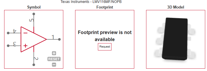
LMV116MF/NOPB ECAD MODELS
|
LMV116MF/NOPB APPLICATIONS
|
|
PARAMETRIC INFO
|
| Manufacturer Type |
Low Voltage Amplifier |
| Type |
Low Voltage Amplifier |
| Rail to Rail |
Rail to Rail Output |
| Minimum Single Supply Voltage (V) |
2.5 |
| Number of Channels per Chip |
1 |
| Process Technology |
Bipolar |
| Minimum PSRR (dB) |
72 |
| Typical Single Supply Voltage (V) |
3|5|9 |
| Maximum Single Supply Voltage (V) |
12 |
| Minimum Dual Supply Voltage (V) |
±1.25 |
| Typical Gain Bandwidth Product (MHz) |
45 |
| Maximum Input Offset Voltage (mV) |
5@5V |
| Typical Dual Supply Voltage (V) |
±3|±5 |
| Maximum Input Offset Current (uA) |
0.5@5V |
| Maximum Dual Supply Voltage (V) |
±6 |
| Maximum Operating Supply Voltage (V) |
±6|12 |
| Maximum Input Bias Current (uA) |
2(Min)@2.7V |
| Minimum CMRR (dB) |
77 |
| Maximum Supply Voltage Range (V) |
12 to 12.5 |
| Minimum CMRR Range (dB) |
75 to 80 |
| Typical Voltage Gain (dB) |
85 |
| Typical Slew Rate (V/us) |
40@5V |
| Typical Output Current (mA) |
20@5V |
| Typical Input Noise Voltage Density (nV/rtHz) |
60@5V |
| Typical Noninverting Input Current Noise Density (pA/rtHz) |
1.2@5V |
| Typical Input Bias Current (uA) |
0.4@5V |
| Shut Down Support |
No |
| Minimum Operating Temperature (°C) |
-40 |
| Maximum Operating Temperature (°C) |
85 |
| Power Supply Type |
Single|Dual |
| Maximum Supply Current (mA) |
0.9@5V |
|
|
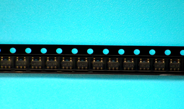
PACKAGE INFO
|
| Supplier Package |
SOT-23 |
| Basic Package Type |
Lead-Frame SMT |
| Pin Count |
5 |
| Lead Shape |
Gull-wing |
| PCB |
5 |
| Tab |
N/R |
| Pin Pitch (mm) |
0.95 |
| Package Length (mm) |
3.05(Max) |
| Package Width (mm) |
1.75(Max) |
| Package Height (mm) |
1.1 |
| Package Diameter (mm) |
N/R |
| Package Overall Length (mm) |
3.05(Max) |
| Package Overall Width (mm) |
3(Max) |
| Package Overall Height (mm) |
1.45(Max) |
| Seated Plane Height (mm) |
1.45(Max) |
| Mounting |
Surface Mount |
| Package Weight (g) |
N/A |
| Package Material |
Plastic |
| Package Description |
Small Outline Transistor |
| Package Family Name |
SOT |
| Jedec |
MO-178AA |
| Package Outline |
Link to Datasheet |
|
|
MANUFACTURING INFO
|
| MSL |
1 |
| Maximum Reflow Temperature (°C) |
260 |
| Reflow Solder Time (Sec) |
30 |
| Number of Reflow Cycle |
3 |
| Standard |
J-STD-020D |
| Reflow Temp. Source |
Link to Datasheet |
| Maximum Wave Temperature (°C) |
N/R |
| Wave Solder Time (Sec) |
N/R |
| Lead Finish(Plating) |
Matte Sn |
| Under Plating Material |
N/A |
| Terminal Base Material |
Cu Alloy |
|
|
PACKAGING INFO
|
| Packaging |
Tape and Reel |
| Quantity Of Packaging |
1000 |
|
|
ECAD MODELS
|
|
|
APPLICATIONS
|
• High-Speed Clock Buffer/Driver
|
| • Active Filters
|
• High-Speed Portable Devices
|
• Multiplexing Applications (LMV118)
|
• Current Sense Amplifier
|
| • High-Speed Transducer Amplifier |
| |