|
| |
• Supply Current 150μA (Max per Amplifi er)Guaranteed from –40°C to 85°C
|
• Offset Voltage 3μV (Max, –40°C to 85°C)
|
• Offset Voltage Drift 30nV/°C (Max, –40°C to 85°C)
|
| • Guaranteed Specifi cations from –55°C to 150°C(LTC2054MP)
|
| • Common Mode Input Range from V– to V+ – 0.5V |
| • Output Swings Rail-to-Rail |
| • Voltage Gain: 140dB (Typ) |
• See TLVH431 and TLVH432 for:– Wider VKA (1.24V to 18 V) and IK (80mA)– Additional SOT-89 package– Multiple pinouts for SOT-23-3 and SOT-89
packages |
| • PSRR and CMRR: 130dB (Typ) |
| • Input Bias Current: 1pA (Typ, 25°C) |
| • Noise: 1.6μVP-P (0.01Hz to 10Hz Typ) |
| • Supply Operation:2.7V to 6V (LTC2054/LTC2055)2.7V to ±5.5V (LTC2054HV/LTC2055HV) |
| • Low Profi le (1mm) TSOT-23, MS8 and3mm × 3mm × 0.8mm DFN Packages |
| |
| CATALOG |
| LTC2055IMS8#TRPBF COUNTRY OF ORIGIN |
LTC2055IMS8#TRPBF PARAMETRIC INFO
|
LTC2055IMS8#TRPBF PACKAGE INFO
|
LTC2055IMS8#TRPBF MANUFACTURING INFO
|
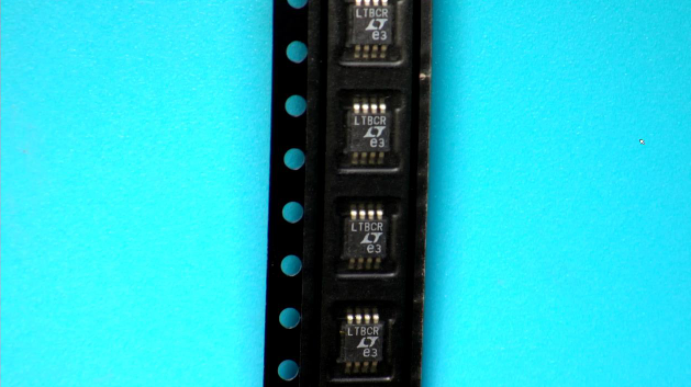
LTC2055IMS8#TRPBF PACKAGING INFO
|
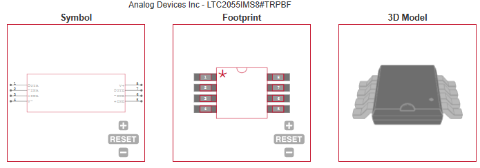
LTC2055IMS8#TRPBF EACD MODELS
|
| LTC2055IMS8#TRPBF APPLICATIONS |
|
| COUNTRY OF ORIGIN |
| Malaysia |
| Thailand |
|
PARAMETRIC INFO
|
| Manufacturer Type |
Zero Drift Amplifier |
| Type |
Zero Drift Amplifier |
| Rail to Rail |
Rail to Rail Output |
| Minimum Single Supply Voltage (V) |
2.7 |
| Number of Channels per Chip |
2 |
| Minimum PSRR (dB) |
120 |
| Typical Single Supply Voltage (V) |
3|5 |
| Maximum Single Supply Voltage (V) |
6 |
| Maximum Quiescent Current (mA) |
0.3@5V@-40C to 85C |
| Typical Gain Bandwidth Product (MHz) |
0.5 |
| Maximum Input Offset Voltage (mV) |
0.003@5V |
| Maximum Input Offset Current (uA) |
0.0003@5V@-40C to 85C |
| Maximum Operating Supply Voltage (V) |
6 |
| Maximum Input Bias Current (uA) |
0.00015@5V@-40C to 85C |
| Minimum CMRR (dB) |
120 |
| Maximum Supply Voltage Range (V) |
6 to 9 |
| Minimum CMRR Range (dB) |
>=115 |
| Typical Voltage Gain (dB) |
140 |
| Typical Slew Rate (V/us) |
0.5@5V |
| Typical Input Offset Current (uA) |
0.000002@5V |
| Typical Input Bias Current (uA) |
0.000001@5V |
| Shut Down Support |
No |
| Minimum Operating Temperature (°C) |
-40 |
| Maximum Operating Temperature (°C) |
85 |
| Supplier Temperature Grade |
Industrial |
| Power Supply Type |
Single |
|
|
PACKAGE INFO
|
| Supplier Package |
MSOP |
| Basic Package Type |
Lead-Frame SMT |
| Pin Count |
8 |
| Lead Shape |
Gull-wing |
| PCB |
8 |
| Tab |
N/R |
| Pin Pitch (mm) |
0.65 |
| Package Length (mm) |
3 |
| Package Width (mm) |
3 |
| Package Height (mm) |
0.86 |
| Package Diameter (mm) |
N/R |
| Package Overall Length (mm) |
3 |
| Package Overall Width (mm) |
4.9 |
| Package Overall Height (mm) |
1.1(Max) |
| Seated Plane Height (mm) |
1.1(Max) |
| Mounting |
Surface Mount |
| Package Weight (g) |
N/A |
| Package Material |
Plastic |
| Package Description |
Micro Small Outline Package |
| Package Family Name |
SO |
| Jedec |
MO-187AA |
| Package Outline |
Link to Datasheet |
|
|
MANUFACTURING INFO
|
| MSL |
1 |
| Maximum Reflow Temperature (°C) |
260 |
| Reflow Solder Time (Sec) |
30 |
| Number of Reflow Cycle |
3 |
| Standard |
J-STD-020D |
| Reflow Temp. Source |
Link to Datasheet |
| Maximum Wave Temperature (°C) |
230 to 250 |
| Wave Solder Time (Sec) |
2 |
| Wave Temp. Source |
Link to Datasheet |
| Lead Finish(Plating) |
Matte Sn annealed |
| Under Plating Material |
Ag |
| Terminal Base Material |
Cu Alloy |
|
|
PACKAGING INFO
|
| Packaging Suffix |
TR |
| Packaging |
Tape and Reel |
| Quantity Of Packaging |
2500 |
| Reel Diameter (in) |
13 |
| Reel Width (mm) |
12.4 |
| Tape Pitch (mm) |
8 |
| Tape Width (mm) |
12 |
| Feed Hole Pitch (mm) |
4 |
| Hole Center to Component Center (mm) |
2 |
| Component Orientation |
Q1 |
| Packaging Document |
Link to Datasheet |
|
|
ECAD MODELS
|
|
|
| APPLICATIONS |
| • Thermocouple Amplifi ers |
| • Electronic Scales |
| • Medical Instrumentation |
| • Strain Gauge Amplifi ers |
• High Resolution Data Acquisition
|
| • DC Accurate RC Active Filters |
| • Low Side Current Sense |
| • Battery-Powered Systems |
| |