|
|
• Passes Automotive AEC-Q100 Reliability Testing
|
• 2.0 µA Quiescent Current (typical)
|
• Input Operating Voltage Range: 2.7V to 13.2V
|
• 250 mA Output Current for Output Voltages 2.5V
|
• 200 mA Output Current for Output Voltages < 2.5V
|
• Low Dropout (LDO) Voltage- 625 mV typical @ 250 mA (VOUT = 2.8V)
|
• 0.4% Typical Output Voltage Tolerance
|
• Standard Output Voltage Options:- 1.2V, 1.5V, 1.8V, 2.5V, 2.8V,
3.0V, 3.3V, 4.0V, 5.0V
|
• Output Voltage Range 1.2V to 5.5V in 0.1V Increments (50 mV increments available upon
request)
|
• Stable with 1.0 µF to 22 µF Output Capacitor
|
• Short-Circuit Protection
|
• Overtemperature Protection
|
|
| CATALOG |
| MCP1702T-2502E/CB COUNTRY OF ORIGIN |
MCP1702T-2502E/CB PARAMETRIC INFO
|
MCP1702T-2502E/CB PACKAGE INFO
|
MCP1702T-2502E/CB MANUFACTURING INFO
|
MCP1702T-2502E/CB PACKAGING INFO
|
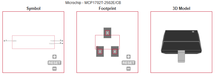
MCP1702T-2502E/CB ECAD MODELS
|
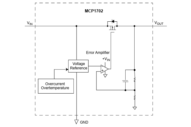
MCP1702T-2502E/CB FUNCTIONAL BLOCK DIAGRAM
|
MCP1702T-2502E/CB APPLICATIONS
|
|
COUNTRY OF ORIGIN
|
| China |
Taiwan (Province of China)
|
Thailand
|
|
PARAMETRIC INFO
|
| Type |
LDO |
| Number of Outputs |
1 |
| Maximum Output Current (A) |
0.25(Min) |
| Minimum Operating Temperature (°C) |
-40 |
| Maximum Operating Temperature (°C) |
125 |
| Output Type |
Fixed |
| Output Voltage Range (V) |
1.8 to 10 |
| Junction to Ambient |
336°C/W(Typ) |
| Junction to Case |
110°C/W(Typ) |
| Polarity |
Positive |
| Special Features |
Current Limit|Short Circuit Protection|Thermal Shutdown Protection |
| Load Regulation |
1%(Typ) |
| Line Regulation |
0.1%/V(Typ) |
| Maximum Quiescent Current (mA) |
0.005 |
| Maximum Dropout Voltage @ Current (V) |
1.1@250mA |
| Minimum Input Voltage (V) |
2.7 |
| Maximum Input Voltage (V) |
13.2 |
| Output Voltage (V) |
2.5 |
| Typical Quiescent Current (mA) |
0.002 |
| Typical Dropout Voltage @ Current (V) |
0.75@250mA |
| Accuracy (%) |
±2 |
| Supplier Temperature Grade |
Extended |
| Minimum Storage Temperature (°C) |
-65 |
| Maximum Storage Temperature (°C) |
150 |
| Noise Spectral Density (uV/rtHz) |
8@1kHz |
| Typical PSRR (dB) |
44 |
| Typical Output Capacitance (uF) |
1 |
| Pass Element Type |
PMOS |
| Output Capacitor Type |
Ceramic |
|
|
PACKAGE INFO
|
| Supplier Package |
SOT-23A |
| Pin Count |
3 |
| PCB |
3 |
| Tab |
N/R |
| Package Length (mm) |
3.1(Max) |
| Package Width (mm) |
1.8(Max) |
| Package Height (mm) |
1.3(Max) |
| Package Diameter (mm) |
N/R |
| Mounting |
Surface Mount |
| Package Outline |
Link to Datasheet |
|
|
MANUFACTURING INFO
|
| MSL |
1 |
| Maximum Reflow Temperature (°C) |
260 |
| Reflow Solder Time (Sec) |
20 to 40 |
| Number of Reflow Cycle |
3 |
| Standard |
J-STD-020C |
| Reflow Temp. Source |
Link to Datasheet |
| Maximum Wave Temperature (°C) |
N/R |
| Wave Solder Time (Sec) |
N/R |
| Lead Finish(Plating) |
Matte Sn annealed |
| Under Plating Material |
N/A |
| Terminal Base Material |
Cu Alloy |
|
|
PACKAGING INFO
|
| Packaging Suffix |
T |
| Packaging |
Tape and Reel |
| Quantity Of Packaging |
3000 |
| Reel Diameter (in) |
7 |
| Tape Pitch (mm) |
4 |
| Tape Width (mm) |
8 |
| Component Orientation |
Single Pin At Sprocket Hole |
| Packaging Document |
Link to Datasheet |
| Tape Type |
Embossed |
|
|
ECAD MODELS
|
|
|
FUNCTIONAL BLOCK DIAGRAM
|
|
|
APPLICATIONS
|
• Battery-powered Devices
|
• Battery-powered Alarm Circuits
|
• Smoke Detectors
|
• CO2 Detectors
|
• Pagers and Cellular Phones
|
• Smart Battery Packs
|
• Low Quiescent Current Voltage Reference
|
• PDAs
|
• Digital Cameras
|
• Microcontroller Power
|
• Solar-Powered Instruments
|
• Consumer Products
|
• Battery Powered Data Loggers
|
| |