|
|
■ Dual TVS in Common Anode Configuration
|
■ 24W/40W Peak Power Dissipation Rating @ 1.0ms
(Unidirectional)
|
■ 225mW Power Dissipation
|
■ Ideally Suited for Automated Insertion
|
■ Low Leakage
|
■ Totally Lead-Free & Fully RoHS Compliant (Notes 1 & 2)
|
■ Halogen and Antimony Free. “Green” Device (Note 3)
|
■ Qualified to AEC-Q101 Standards for High Reliability
|
|
| CATALOG |
| MMBZ6V8AL-7-F COUNTRY OF ORIGIN |
MMBZ6V8AL-7-F LIFECYCLE
|
MMBZ6V8AL-7-F PARAMETRIC INFO
|
MMBZ6V8AL-7-F PACKAGE INFO
|
MMBZ6V8AL-7-F MANUFACTURING INFO
|
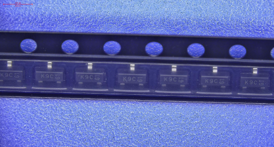
| MMBZ6V8AL-7-F PACKAGING INFO
|
|
COUNTRY OF ORIGIN
|
China
|
|
LIFECYCLE
|
Obsolete
Sep 15,2021
|
|
PARAMETRIC INFO
|
| Type |
Zener |
| Direction Type |
Uni-Directional|Bi-Directional |
| Maximum Working Voltage (V) |
4.5 |
| Maximum Power Dissipation (mW) |
225 |
| Nominal Zener Voltage (V) |
6.8 |
| Configuration |
Dual Common Anode|Single |
| Maximum Clamping Voltage (V) |
9.6 |
| Maximum Leakage Current (uA) |
0.5 |
| Operating Junction Temperature (°C) |
-65 to 150 |
| Number of Elements per Chip |
2 |
| Maximum Breakdown Voltage (V) |
7.14 |
| Test Current (mA) |
1 |
| Peak Pulse Power Dissipation (W) |
24 |
| Maximum Peak Pulse Current (A) |
2.5 |
| Minimum Breakdown Voltage (V) |
6.46 |
| Minimum Operating Temperature (°C) |
-65 |
| Fail Safe Protection |
No |
| Maximum Operating Temperature (°C) |
150 |
| Minimum Storage Temperature (°C) |
-65 |
| Maximum Storage Temperature (°C) |
150 |
| Supplier Temperature Grade |
Commercial |
|
|
PACKAGE INFO
|
| Supplier Package |
SOT-23 |
| Basic Package Type |
Lead-Frame SMT |
| Pin Count |
3 |
| Lead Shape |
Gull-wing |
| PCB |
3 |
| Tab |
N/R |
| Pin Pitch (mm) |
0.92 |
| Package Length (mm) |
2.9 |
| Package Width (mm) |
1.3 |
| Package Height (mm) |
0.98 |
| Package Diameter (mm) |
N/R |
| Package Overall Length (mm) |
2.9 |
| Package Overall Width (mm) |
2.4 |
| Package Overall Height (mm) |
1.03 |
| Seated Plane Height (mm) |
1.03 |
| Mounting |
Surface Mount |
| Package Weight (g) |
N/A |
| Package Material |
Plastic |
| Package Description |
Small Outline Transistor |
| Package Family Name |
SOT |
| Jedec |
TO-236AA |
| Package Outline |
Link to Datasheet |
|
|
MANUFACTURING INFO
|
| MSL |
1 |
| Maximum Reflow Temperature (°C) |
260 |
| Reflow Solder Time (Sec) |
30 |
| Number of Reflow Cycle |
3 |
| Standard |
J-STD-020D |
| Reflow Temp. Source |
Link to Datasheet |
| Maximum Wave Temperature (°C) |
N/R |
| Wave Solder Time (Sec) |
N/R |
| Lead Finish(Plating) |
Matte Sn annealed |
| Under Plating Material |
N/A |
| Terminal Base Material |
Alloy 42 |
|
|
PACKAGING INFO
|
| Packaging Suffix |
7 |
| Packaging |
Tape and Reel |
| Quantity Of Packaging |
3000 |
| Reel Diameter (in) |
7 |
| Reel Width (mm) |
8.4 |
| Tape Pitch (mm) |
4 |
| Tape Width (mm) |
8 |
| Feed Hole Pitch (mm) |
4 |
| Hole Center to Component Center (mm) |
2 |
| Component Orientation |
Single Pin At Sprocket Hole |
| Packaging Document |
Link to Datasheet |
| Tape Type |
Embossed |
|
|