|
|
• 3.3 V, 5.0 V Fixed Output
|
• ±2.0% Output Accuracy, Over Full Temperature Range
|
• 30 A Maximum Quiescent Current at IOUT = 100 A
|
• 600 mV Maximum Dropout Voltage at 150 mA Load Current
|
• Wide Input Voltage Operating Range of 4.5 V to 45 V
|
• Internal Fault Protection♦ −42 V Reverse Voltage♦ Short Circuit/Overcurrent♦ Thermal Overload
|
• NCV Prefix for Automotive and Other Applications Requiring Unique Site and Control Change Requirements; AEC−Q100 Qualified and PPAP Capable
|
• EMC Compliant
|
• These are Pb−Free Devices
|
|
| CATALOG |
NCV8664ST50T3G COUNTRY OF ORIGIN
|
NCV8664ST50T3G PARAMETRIC INFO
|
NCV8664ST50T3G PACKAGE INFO
|
NCV8664ST50T3G MANUFACTURING INFO
|
NCV8664ST50T3G PACKAGING INFO
|
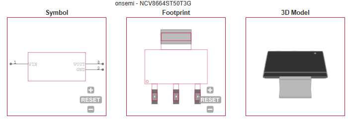
NCV8664ST50T3G ECAD MODELS
|
|
COUNTRY OF ORIGIN
|
Malaysia
|
|
PARAMETRIC INFO
|
| Type |
LDO |
| Number of Outputs |
1 |
| Maximum Output Current (A) |
0.15 |
| Minimum Operating Temperature (°C) |
-40 |
| Maximum Operating Temperature (°C) |
150 |
| Output Type |
Fixed |
| Output Voltage Range (V) |
1.8 to 10 |
| Junction to Ambient |
99°C/W |
| Junction to Case |
17°C/W |
| Polarity |
Positive |
| Special Features |
Current Limit|Fault Protection|Short Circuit Protection|Thermal Protection |
| Load Regulation |
35mV |
| Line Regulation |
25mV |
| Maximum Quiescent Current (mA) |
0.029 |
| Maximum Dropout Voltage @ Current (V) |
0.5@100mA|0.6@150mA |
| Minimum Input Voltage (V) |
4.5 |
| Maximum Input Voltage (V) |
45 |
| Output Voltage (V) |
5 |
| Typical Quiescent Current (mA) |
0.021 |
| Typical Dropout Voltage @ Current (V) |
0.265@100mA|0.315@150mA |
| Reference Voltage (V) |
1.3 |
| Accuracy (%) |
±2 |
| Supplier Temperature Grade |
Automotive |
|
|
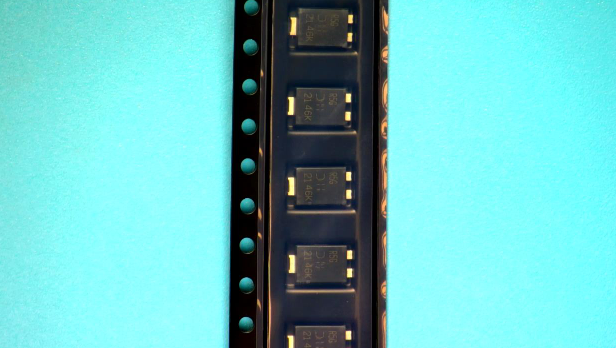
PACKAGE INFO
|
| Supplier Package |
SOT-223 |
| Basic Package Type |
Lead-Frame SMT |
| Pin Count |
4 |
| Lead Shape |
Gull-wing |
| PCB |
3 |
| Tab |
Tab |
| Pin Pitch (mm) |
2.3 |
| Package Length (mm) |
6.5 |
| Package Width (mm) |
3.5 |
| Package Height (mm) |
1.57 |
| Package Diameter (mm) |
N/R |
| Package Overall Length (mm) |
6.5 |
| Package Overall Width (mm) |
7 |
| Package Overall Height (mm) |
1.63 |
| Seated Plane Height (mm) |
1.63 |
| Mounting |
Surface Mount |
| Package Weight (g) |
N/A |
| Package Material |
Plastic |
| Package Description |
Small Outline Transistor |
| Package Family Name |
SOT |
| Jedec |
TO-261AA |
| Package Outline |
Link to Datasheet |
|
|
MANUFACTURING INFO
|
| MSL |
3 |
| Maximum Reflow Temperature (°C) |
260 |
| Reflow Solder Time (Sec) |
20 to 40 |
| Number of Reflow Cycle |
3 |
| Standard |
J-STD-020C |
| Reflow Temp. Source |
Link to Datasheet |
| Maximum Wave Temperature (°C) |
N/R |
| Wave Solder Time (Sec) |
N/R |
| Lead Finish(Plating) |
Matte Sn annealed |
| Under Plating Material |
N/A |
| Terminal Base Material |
CuFeAgZn |
|
|
PACKAGING INFO
|
| Packaging Suffix |
T3 |
| Packaging |
Tape and Reel |
| Quantity Of Packaging |
4000 |
| Packaging Document |
Link to Datasheet |
|
|
| ECAD MODELS |
 |
| |