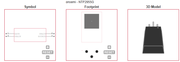
| Channel Type |
P |
| Channel Mode |
Enhancement |
| Configuration |
Single |
| Maximum Drain Source Voltage (V) |
60 |
| Maximum Continuous Drain Current (A) |
2.4 |
| Maximum Gate Source Voltage (V) |
±20 |
| Maximum Drain Source Resistance (mOhm) |
196@10V |
| Typical Gate Charge @ Vgs (nC) |
14@10V |
| Typical Gate Charge @ 10V (nC) |
14 |
| Maximum Power Dissipation (mW) |
2400 |
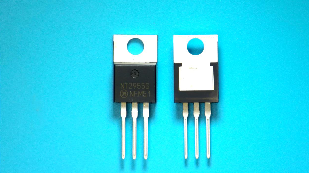
| Category |
Power MOSFET |
| Typical Input Capacitance @ Vds (pF) |
507@25V |
| Typical Turn-On Delay Time (ns) |
10 |
| Typical Turn-Off Delay Time (ns) |
27 |
| Typical Fall Time (ns) |
45 |
| Typical Rise Time (ns) |
41 |
| Number of Elements per Chip |
1 |
| Minimum Operating Temperature (°C) |
-55 |
| Maximum Operating Temperature (°C) |
175 |