|
|
• 1-of-8 Bidirectional Translating Switches
|
• I2C Bus and SMBus Compatible
|
• Active-Low Reset Input
|
| • Three Hardware Address Pins for Use of up to Eight PCA9548A Devices on the I2C Bus
|
| • Channel Selection Via I2C Bus |
| • Power-Up with All Switch Channels Deselected |
| • Low RON Switches |
| • Allows Voltage-Level Translation Between 1.8-V, 2.5-V, 3.3-V, and 5-V Buses |
| • No Glitch on Power Up |
| • Supports Hot Insertion |
| • Low Standby Current |
| • Operating Power-Supply Voltage Range of 2.3 V to 5.5 V |
| • 5-V Tolerant Inputs |
|
| CATALOG |
| PCA9548APWR COUNTRY OF ORIGIN |
PCA9548APWR PARAMETRIC INFO
|
PCA9548APWR PACKAGE INFO
|
PCA9548APWR MANUFACTURING INFO
|
PCA9548APWR PACKAGING INFO
|
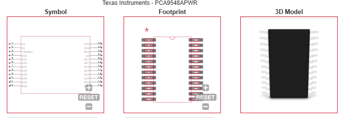
PCA9548APWR ECAD MODELS
|
| PCA9548APWR APPLICATIONS |
|
| COUNTRY OF ORIGIN |
| Malaysia |
China
|
| Taiwan (Province of China) |
| Philippines |
|
PARAMETRIC INFO
|
| Logic Function |
I2C Bus Switch |
| Number of Elements per Chip |
1 |
| Number of Inputs per Chip |
8 |
| Number of Outputs per Chip |
1 |
| Configuration |
1 x 8:1 |
| Maximum On Resistance (Ohm) |
15(Typ) |
| Minimum Operating Supply Voltage (V) |
2.3 |
| Maximum Operating Supply Voltage (V) |
5.5 |
| Typical Operating Supply Voltage (V) |
2.5|3.3|5 |
| Minimum Operating Temperature (°C) |
-40 |
| Maximum Operating Temperature (°C) |
85 |
| Maximum Propagation Delay Time @ Maximum CL (ns) |
0.3@2.3V to 5.5V |
| Absolute Propagation Delay Time (ns) |
0.3 |
| Propagation Delay Test Condition (pF) |
50 |
| Maximum Low Level Output Current (mA) |
9(Typ) |
| Maximum Quiescent Current (uA) |
80 |
| Typical Quiescent Current (uA) |
50 |
|
|
PACKAGE INFO
|
| Supplier packaging |
TSSOP |
| Basic package type |
Lead-Frame SMT |
| Number of pins |
twenty four |
| Pin shape |
Gull-wing |
| PCB |
twenty four |
| ears |
N/R |
| Pin spacing (mm) |
0.65 |
| Package length (mm) |
7.9(Max) |
| Package width (mm) |
4.5(Max) |
| Package height (mm) |
1.05(Max) |
| Package diameter (mm) |
N/R |
| Package Overall Length (mm) |
7.9(Max) |
| Package Overall Width (mm) |
6.6(Max) |
| Package Overall Height (mm) |
1.2(Max) |
| Mounting surface height (mm) |
1.2(Max) |
| Install |
Surface Mount |
| Package weight (g) |
not applicable |
| Packaging materials |
Plastic |
| package instruction |
Thin Shrink Small Outline Package |
| Package series name |
SO |
| JEDEC |
MO-153AD |
| Package outline |
Link to datasheet |
|
|
MANUFACTURING INFO
|
| MSL |
1 |
| Maximum reflow temperature (°C) |
260 |
| Reflow soldering time (seconds) |
30 |
| Number of reflow cycles |
3 |
| standard |
J-STD-020D |
| Reflow temperature source |
Link to datasheet |
| Maximum wave soldering temperature (°C) |
N/R |
| Wave soldering time (seconds) |
N/R |
| Lead Finish(Plating) |
Au |
| Plating materials |
Pd over Ni |
| Terminal Base Material |
Cu Alloy |
| Number of Wave Cycles |
N/R |
|
|
PACKAGING INFO
|
| Packaging Suffix |
R |
| Package |
Tape and reel packaging |
| Packing quantity |
2000 |
| Reel Diameter (in) |
13 |
| Reel Width (mm) |
16.4 |
| Tape Pitch (mm) |
8 |
| Tape Width (mm) |
16 |
| Component Orientation |
Q1 |
| packaging type file |
Link to datasheet |
|
|
ECAD MODELS
|
|
|
APPLICATIONS
|
• Servers
|
| • Routers (Telecom Switching Equipment) |
| • Factory Automation |
| • Products With I2C Slave Address Conflicts (For Example, Multiple, Identical Temp Sensors) |
| |
| |