|
| |
• High isolation voltage (BV = 2 500 Vr.m.s.)
|
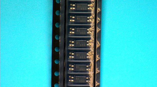
• Small and thin package (4,16-pin SSOP, Pin pitch 1.27 mm)
|
• High collector to emitter voltage (VCEO = 80 V)
|
| • High-speed switching (tr = 3 s TYP., tf = 5 s TYP.)
|
| • Ordering number of tape product: PS2801-1-F3, PS2801-4-F3 |
| • Pb-Free product |
| • Safety standards UL approved: UL1577, Single protection CSA approved: CAN/CSA-C22.2 No. 62368-1, Basic insulation BSI approved: BS EN 62368-1, Basic/Supplementary insulation VDE approved: DIN EN 60747-5-5 (Option) |
| |
| CATALOG |
| PS2801-1-F3-A COUNTRY OF ORIGIN |
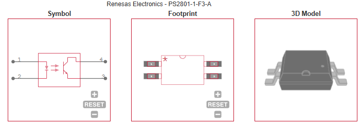
PS2801-1-F3-A PARAMETRIC INFO
|
PS2801-1-F3-A PACKAGE INFO
|
PS2801-1-F3-A MANUFACTURING INFO
|
PS2801-1-F3-A PACKAGING INFO
|
PS2801-1-F3-A EACD MODELS
|
| PS2801-1-F3-A APPLICATIONS |
|
| COUNTRY OF ORIGIN |
| Taiwan (Province of China) |
|
PARAMETRIC INFO
|
| Input Type |
DC |
| Output Type |
DC |
| Output Device |
Transistor |
| Standard |
BSI|CSA|UL |
| Number of Channels per Chip |
1 |
| Typical Forward Voltage (V) |
1.1 |
| Maximum Forward Voltage (V) |
1.4 |
| Maximum Forward Current (mA) |
50/ch |
| Maximum Collector Current (mA) |
50/ch |
| Maximum Reverse Voltage (V) |
6 |
| Maximum Collector-Emitter Voltage (V) |
80 |
| Maximum Collector-Emitter Saturation Voltage (mV) |
300 |
| Minimum Isolation Voltage (Vrms) |
2500 |
| Maximum Power Dissipation (mW) |
120/ch |
| Minimum Current Transfer Ratio (%) |
80 |
| Maximum Current Transfer Ratio (%) |
600 |
| Current Transfer Ratio Test Current (mA) |
5 |
| Typical Rise Time (us) |
3 |
| Typical Fall Time (us) |
5 |
| Minimum Operating Temperature (°C) |
-55 |
| Maximum Operating Temperature (°C) |
100 |
| Maximum Storage Temperature (°C) |
150 |
| Minimum Storage Temperature (°C) |
-55 |
|
|
PACKAGE INFO
|
| Supplier Package |
SSOP |
| Basic Package Type |
Lead-Frame SMT |
| Pin Count |
4 |
| Lead Shape |
Gull-wing |
| PCB |
4 |
| Tab |
N/R |
| Pin Pitch (mm) |
1.27 |
| Package Length (mm) |
2.7 |
| Package Width (mm) |
4.4 |
| Package Height (mm) |
1.9 |
| Package Diameter (mm) |
N/R |
| Seated Plane Height (mm) |
2 |
| Mounting |
Surface Mount |
| Package Weight (g) |
N/A |
| Package Material |
Plastic |
| Package Description |
Shrink Small Outline Package |
| Package Family Name |
SO |
| Jedec |
N/A |
|
|
MANUFACTURING INFO
|
| MSL |
1 |
| Maximum Reflow Temperature (°C) |
260 |
| Reflow Solder Time (Sec) |
10 |
| Number of Reflow Cycle |
3 |
| Standard |
N/A |
| Reflow Temp. Source |
Link to Datasheet |
| Maximum Wave Temperature (°C) |
260 |
| Wave Solder Time (Sec) |
10 |
| Wave Temp. Source |
Link to Datasheet |
| Lead Finish(Plating) |
SnBi |
| Under Plating Material |
N/A |
| Terminal Base Material |
N/A |
| Number of Wave Cycles |
1 |
|
|
PACKAGING INFO
|
|
|
|
ECAD MODELS
|
|
|
| APPLICATIONS |
| • Programmable logic controllers |
| • Measuring instruments |
| • Power supply |
| • Hybrid IC |
|
| |