|
|
• Wide range of trip and non-trip currents: From 94 mA up to 2 A for the trip current
|
• Small ratio between trip and non-trip currents(It/Int = 1.5 at 25 °C)
|
• High maximum overload current (up to 23 A)
|
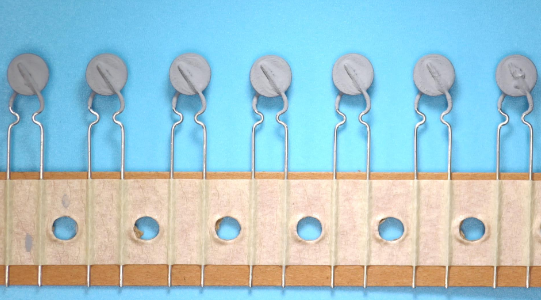
• Leaded parts withstand mechanical stresses and vibration
|
• UL file E148885 according to XGPU standard UL1434
|
• Material categorization: for definitions of compliance please see www.vishay.com/doc?99912
|
|
| CATALOG |
PTCCL07H411DTE PARAMETRIC INFO
|
PTCCL07H411DTE PACKAGE INFO
|
PTCCL07H411DTE MANUFACTURING INFO
|
PTCCL07H411DTE PACKAGING INFO
|
PTCCL07H411DTE APPLICATIONS
|
|
PARAMETRIC INFO
|
| Type |
PTC |
| Resistance Range @ 25C (Ohm) |
< 7 |
| Percentage of Resistance Tolerance Range @ 25C (%) |
±20 to ±25 |
| Resistance @ 25C (Ohm) |
3 |
| Percentage of Resistance Tolerance @ 25C (%) |
±20 |
| Maximum Voltage Rating |
30VDC|30VAC |
| Application |
Telecommunication|Automotive System|Industrial Electronic|Consumer Electronic |
| Description of Terminals |
0.6mm dia. x 20mm Inside Crimp Standoff |
| Maximum Operating Temperature (°C) |
85 |
| Minimum Operating Temperature (°C) |
-40 |
| Lead Diameter (mm) |
0.6 |
| Lead Length (mm) |
20 |
| Wire Form |
Inside Crimp Standoff |
| Construction |
Radial |
|
|
PACKAGE INFO
|
| Mounting |
Through Hole |
| Terminal Pitch (mm) |
5 |
| Package/Case |
N/A |
| Number of Terminals |
2 |
| Product Length (mm) |
N/R |
| Product Depth (mm) |
4(Max) |
| Product Height (mm) |
N/R |
| Product Diameter (mm) |
7(Max) |
| Seated Plane Height (mm) |
12(Max) |
| Maximum Product Depth (mm) |
4 |
|
|
MANUFACTURING INFO
|
| MSL |
1 |
| Maximum Reflow Temperature (°C) |
260 |
| Reflow Solder Time (Sec) |
30 |
| Number of Reflow Cycle |
3 |
| Maximum Wave Temperature (°C) |
260 |
| Wave Solder Time (Sec) |
10 |
| Wave Temp. Source |
Link to Datasheet |
| Lead Finish(Plating) |
Sn |
| Under Plating Material |
Ni |
| Terminal Base Material |
Cu Clad Steel |
|
|
PACKAGING INFO
|
|
|
|
APPLICATIONS
|
• Industrial electronics
|
• Consumer electronics
|
• Electronic data processing
|
|
|