|
| |
• Four ('391), Eight ('389), or Sixteen ('387) Line Drivers Meet or Exceed the Requirements of ANSI EIA/TIA-644 Standard
|
• Designed for Signaling Rates Up to 630 Mbps With Very Low Radiation (EMI)
|
• Low-Voltage Differential Signaling With Typical Output Voltage of 350 mV and a 100-Ω Load
|
| • Propagation Delay Times Less Than 2.9 ns |
| • Output Skew Is Less Than 150 ps |
| • Part-to-Part Skew Is Less Than 1.5 ns |
| • 35-mW Total Power Dissipation in Each Driver Operating at 200 MHz |
| • Driver Is High-Impedance When Disabled or With VCC < 1.5 V |
| • Packaged in Thin Shrink Small-Outline Package With 20-mil Pin Pitch |
| • Low-Voltage TTL (LVTTL) Logic Inputs Are 5-V Tolerant |
| |
| CATALOG |
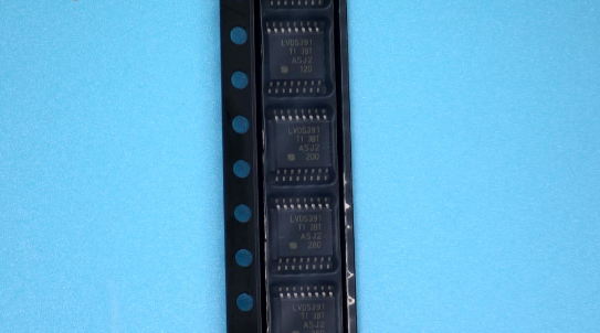
| SN65LVDS391PWR COUNTRY OF ORIGIN |
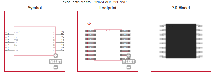
SN65LVDS391PWR PARAMETRIC INFO
|
SN65LVDS391PWR PACKAGE INFO
|
SN65LVDS391PWR MANUFACTURING INFO
|
SN65LVDS391PWR PACKAGING INFO
|
SN65LVDS391PWR EACD MODELS
|
| SN65LVDS391PWR APPLICATIONS |
|
| COUNTRY OF ORIGIN |
| China |
| Taiwan (Province of China) |
| Malaysia |
|
PARAMETRIC INFO
|
| Function |
Driver |
| Number of Drivers |
4 |
| Number of Receivers |
0 |
| Input Signal Type |
LVTTL |
| Transmission Data Rate (Mbps) |
630 |
| Number of Elements per Chip |
16 |
| Minimum Operating Supply Voltage (V) |
3 |
| Typical Operating Supply Voltage (V) |
3.3 |
| Maximum Operating Supply Voltage (V) |
3.6 |
| Maximum Input Current (uA) |
20 |
| Output Signal Type |
LVDS |
| Maximum Differential Output Voltage (V) |
0.454 |
| Maximum Power Dissipation (mW) |
774 |
| Maximum Operating Frequency (MHz) |
200 |
| Maximum Propagation Delay Time (ns) |
2.9 |
| Minimum Operating Temperature (°C) |
-40 |
| Maximum Operating Temperature (°C) |
85 |
| Maximum Storage Temperature (°C) |
150 |
| Minimum Storage Temperature (°C) |
-65 |
|
|
PACKAGE INFO
|
| Supplier Package |
TSSOP |
| Basic Package Type |
Lead-Frame SMT |
| Pin Count |
16 |
| Lead Shape |
Gull-wing |
| PCB |
16 |
| Tab |
N/R |
| Pin Pitch (mm) |
0.65 |
| Package Length (mm) |
5.1(Max) |
| Package Width (mm) |
4.5(Max) |
| Package Height (mm) |
1.05(Max) |
| Package Diameter (mm) |
N/R |
| Package Overall Length (mm) |
5.1(Max) |
| Package Overall Width (mm) |
6.6(Max) |
| Package Overall Height (mm) |
1.2(Max) |
| Seated Plane Height (mm) |
1.2(Max) |
| Mounting |
Surface Mount |
| Package Weight (g) |
N/A |
| Package Material |
Plastic |
| Package Description |
Thin Shrink Small Outline Package |
| Package Family Name |
SO |
| Jedec |
MO-153AB |
| Package Outline |
Link to Datasheet |
|
|
MANUFACTURING INFO
|
| MSL |
1 |
| Maximum Reflow Temperature (°C) |
260 |
| Reflow Solder Time (Sec) |
30 |
| Number of Reflow Cycle |
3 |
| Standard |
J-STD-020D |
| Reflow Temp. Source |
Link to Datasheet |
| Maximum Wave Temperature (°C) |
N/R |
| Wave Solder Time (Sec) |
N/R |
| Lead Finish(Plating) |
Au |
| Under Plating Material |
Pd over Ni |
| Terminal Base Material |
Cu Alloy |
| Number of Wave Cycles |
N/R |
|
|
PACKAGING INFO
|
| Packaging Suffix |
R |
| Packaging |
Tape and Reel |
| Quantity Of Packaging |
2000 |
| Reel Diameter (in) |
13 |
| Reel Width (mm) |
12.4 |
| Tape Pitch (mm) |
8 |
| Tape Width (mm) |
12 |
| Component Orientation |
Q1 |
| Packaging Document |
Link to Datasheet |
|
|
ECAD MODELS
|
|
|
| APPLICATIONS |
| • Wireless Infrastructure |
| • Telecom Infrastructure |
| • Printer |
| |