
|
|
• Available in the Ultra Small 0.64-mm2 Package (DPW) With 0.5-mm Pitch
|
• Inputs Accept Voltages to 5.5 V
|
• Provides Down Translation to VCC
|
• Max tpd of 3.7 ns at 3.3 V
|
•Low Power Consumption, 10-μA Max ICC
|
•±24-mA Output Drive at 3.3 V
|
•Ioff Supports Live Insertion, Partial-Power-Down Mode, and Back-Drive Protection
|
•Latch-Up Performance Exceeds 100 mA Per JESD 78, Class I
|
•ESD Protection Exceeds JESD 22 – 2000-V Human-Body Model (A114-A) – 200-V Machine Model (A115-A) – 1000-V Charged-Device Model (C101)
|
|
| CATALOG |
SN74LVC1G125DCKR COUNTRY OF ORIGIN
|
SN74LVC1G125DCKR PARAMETRIC INFO
|
SN74LVC1G125DCKR PACKAGE INFO
|
SN74LVC1G125DCKR MANUFACTURING INFO
|
SN74LVC1G125DCKR PACKAGING INFO
|
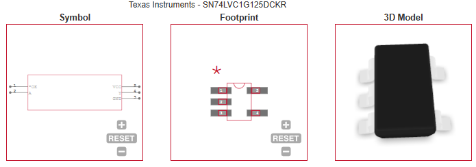
SN74LVC1G125DCKR ECAD MODELS
|
SN74LVC1G125DCKR APPLICATIONS
|
|
COUNTRY OF ORIGIN
|
China
|
Malaysia
|
Taiwan (Province of China)
|
United States of America
|
Thailand
|
|
PARAMETRIC INFO
|
| Process Technology |
CMOS |
| Logic Family |
LVC |
| Logic Function |
Buffer/Line Driver |
| Input Signal Type |
Single-Ended |
| Output Type |
3-State |
| Polarity |
Non-Inverting |
| Tolerant I/Os (V) |
5.5 Inputs |
| Bus Hold |
No |
| Number of Elements per Chip |
1 |
| Number of Channels per Chip |
1 |
| Number of Output Enables per Chip |
1 Low |
| Number of Input Enables per Chip |
0 |
| Number of Inputs per Chip |
1 |
| Number of Outputs per Chip |
1 |
| Minimum Operating Supply Voltage (V) |
1.65 |
| Maximum Operating Supply Voltage (V) |
5.5 |
| Typical Operating Supply Voltage (V) |
1.8|2.5|3.3|5 |
| Minimum Operating Temperature (°C) |
-40 |
| Maximum Operating Temperature (°C) |
125 |
| Minimum Storage Temperature (°C) |
-65 |
| Maximum Storage Temperature (°C) |
150 |
| Maximum Propagation Delay Time @ Maximum CL (ns) |
4.7@3.3V|4.2@5V |
| Absolute Propagation Delay Time (ns) |
10.4 |
| Propagation Delay Test Condition (pF) |
50 |
| Maximum High Level Output Current (mA) |
-32 |
| Maximum Low Level Output Current (mA) |
32 |
| Maximum Quiescent Current (uA) |
10 |
|
|
PACKAGE INFO
|
| Supplier Package |
SC-70 |
| Basic Package Type |
Lead-Frame SMT |
| Pin Count |
5 |
| Lead Shape |
Gull-wing |
| PCB |
5 |
| Tab |
N/R |
| Pin Pitch (mm) |
0.65 |
| Package Length (mm) |
2.15(Max) |
| Package Width (mm) |
1.4(Max) |
| Package Height (mm) |
1(Max) |
| Package Diameter (mm) |
N/R |
| Seated Plane Height (mm) |
1.1(Max) |
| Mounting |
Surface Mount |
| Package Weight (g) |
N/A |
| Package Material |
Plastic |
| Package Description |
Small Outline Transistor |
| Package Family Name |
SOT |
| Jedec |
MO-203AA |
| Package Outline |
Link to Datasheet |
|
|
MANUFACTURING INFO
|
| MSL |
1 |
| Maximum Reflow Temperature (°C) |
260 |
| Reflow Solder Time (Sec) |
30 |
| Number of Reflow Cycle |
3 |
| Standard |
J-STD-020D |
| Reflow Temp. Source |
Link to Datasheet |
| Maximum Wave Temperature (°C) |
N/R |
| Wave Solder Time (Sec) |
N/R |
| Wave Temp. Source |
Link to Datasheet |
| Lead Finish(Plating) |
Matte Sn|Au |
| Under Plating Material |
N/A|Pd over Ni |
| Terminal Base Material |
N/A|Cu Alloy |
| Shelf Life Period |
N/A |
| Shelf Life Condition |
N/A |
| Number of Wave Cycles |
N/R |
|
|
PACKAGING INFO
|
| Packaging Suffix |
R |
| Packaging |
Tape and Reel |
| Quantity Of Packaging |
3000 |
| Reel Diameter (in) |
7 |
| Reel Width (mm) |
8.4|9|9.2 |
| Tape Pitch (mm) |
4 |
| Tape Width (mm) |
8 |
| Component Orientation |
Q3 |
| Packaging Document |
Link to Datasheet |
|
|
ECAD MODELS
|
|
|
APPLICATIONS
|
• Cable Modem Termination System
|
| • High-Speed Data Acquisition and Generation |
• Military: Radar and Sonar
|
• Motor Control: High-Voltage
|
• Power Line Communication Modem
|
• SSD: Internal or Externa
|
| • Video Broadcasting and Infrastructure:
Scalable Platform |
• Video Broadcasting: IP-Based Multi-Format
Transcoder
|
• Video Communications System
|
| |