|
|
• Bidirectional voltage translator
|
• 4.5 V to 5.5 V on A port and
2.7 V to 5.5 V on B port
|
• Control inputs VIH and VIL levels are referenced to
VCCA voltage
|
• Latch-up performance exceeds 250 mA
per JESD 17
|
• ESD protection exceeds JESD 22
– 2000-V Human-Body Model (A114-A)
– 1000-V Charged-Device Model (C101)
|
|
| CATALOG |
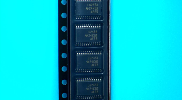
| SN74LVCC4245APWR COUNTRY OF ORIGIN |
SN74LVCC4245APWR PARAMETRIC INFO
|
SN74LVCC4245APWR PACKAGE INFO
|
SN74LVCC4245APWR MANUFACTURING INFO
|
SN74LVCC4245APWR PACKAGING INFO
|
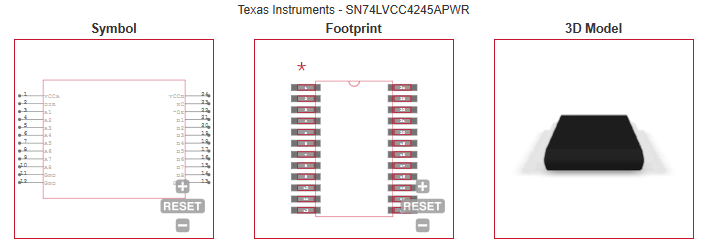
SN74LVCC4245APWR ECAD MODELS
|
SN74LVCC4245APWR APPLICATIONS
|
|
COUNTRY OF ORIGIN
|
Malaysia
|
|
PARAMETRIC INFO
|
| Number of Channels |
8 |
| Channel Type |
Bidirectional |
| Logic Family |
LVC |
| Process Technology |
CMOS |
| Logic Function |
Voltage Level Translator |
| Output Type |
3-State |
| Minimum Operating Temperature (°C) |
-40 |
| Maximum Operating Temperature (°C) |
85 |
| Minimum Operating Supply Voltage (V) |
2.7/4.5 |
| Maximum Operating Supply Voltage (V) |
5.5 |
| Typical Operating Supply Voltage (V) |
3.3/5 |
| Maximum High Level Output Current (mA) |
-24 |
| Maximum Low Level Output Current (mA) |
24 |
| Maximum Quiescent Current (mA) |
0.08 |
| Maximum Propagation Delay Time @ Maximum CL (ns) |
7.1@4.5V to 5.5V |
| Absolute Propagation Delay Time (ns) |
10.2 |
|
|
PACKAGE INFO
|
| Supplier Package |
TSSOP |
| Basic Package Type |
Lead-Frame SMT |
| Pin Count |
24 |
| Lead Shape |
Gull-wing |
| PCB |
24 |
| Tab |
N/R |
| Pin Pitch (mm) |
0.65 |
| Package Length (mm) |
7.9(Max) |
| Package Width (mm) |
4.5(Max) |
| Package Height (mm) |
1.05(Max) |
| Package Diameter (mm) |
N/R |
| Package Overall Length (mm) |
7.9(Max) |
| Package Overall Width (mm) |
6.6(Max) |
| Package Overall Height (mm) |
1.2(Max) |
| Seated Plane Height (mm) |
1.2(Max) |
| Mounting |
Surface Mount |
| Package Material |
Plastic |
| Package Description |
Thin Shrink Small Outline Package |
| Package Family Name |
SOP |
| Jedec |
MO-153AD |
| Package Outline |
Link to Datasheet |
|
|
MANUFACTURING INFO
|
| MSL |
1 |
| Maximum Reflow Temperature (°C) |
260 |
| Reflow Solder Time (Sec) |
30 |
| Number of Reflow Cycle |
3 |
| Standard |
J-STD-020D |
| Reflow Temp. Source |
Link to Datasheet |
| Maximum Wave Temperature (°C) |
N/R |
| Wave Solder Time (Sec) |
N/R |
| Lead Finish(Plating) |
Au |
| Under Plating Material |
Pd over Ni |
| Terminal Base Material |
Cu Alloy |
|
|
PACKAGING INFO
|
| Packaging Suffix |
R |
| Packaging |
Tape and Reel |
| Quantity Of Packaging |
2000 |
| Reel Diameter (in) |
13 |
| Tape Pitch (mm) |
8 |
| Tape Width (mm) |
16 |
| Component Orientation |
Q1 |
| Packaging Document |
Link to Datasheet |
|
|
ECAD MODELS
|
|
|
APPLICATIONS
|
• Level translation
|
• Personal electronics
|
• Industrial
|
• Enterprise
|
• Telecom
|
|