|
|
• Organized as 2M x16
|
• Low Power Consumption (typical values at 5 MHz) – Active Current: 6 mA (typical) – Standby Current: 4 µA (typical)
|
• Hardware Block-Protection/WP# Input Pin – Top Block-Protection (top two 4-KWord blocks) for SST39VF3202C – Bottom BlockProtection for SST39VF3201C
|
• Sector-Erase Capability – Uniform 2 KWord sectors
|
• Block-Erase Capability – Flexible block architecture – Eight 4-KWord blocks, 63 32-KWord blocks
|
• Chip-Erase Capability
|
|
| CATALOG |
SST39VF3201C-70-4I-B3KE PARAMETRIC INFO
|
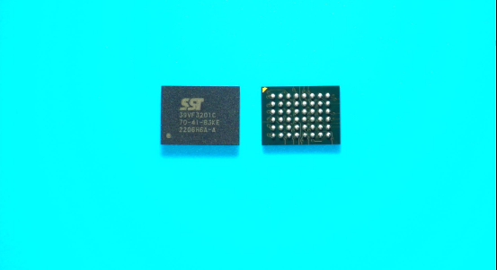
SST39VF3201C-70-4I-B3KE PACKAGE INFO
|
SST39VF3201C-70-4I-B3KE MANUFACTURING INFO
|
SST39VF3201C-70-4I-B3KE PACKAGING INFO
|
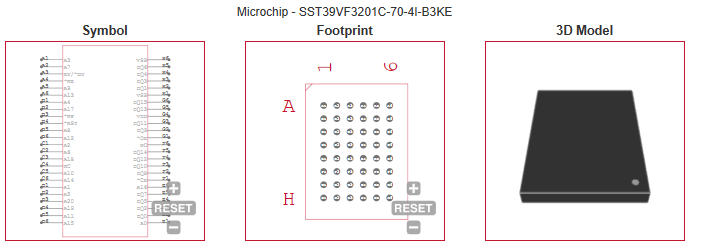
SST39VF3201C-70-4I-B3KE ECAD MODELS
|
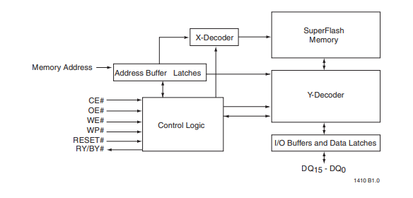
SST39VF3201C-70-4I-B3KE BLOCK DIAGRAM
|
|
PARAMETRIC INFO
|
| Density (bit) |
32M |
| Cell Type |
NOR |
| Interface Type |
Parallel |
| Block Organization |
Symmetrical |
| Boot Block |
Yes |
| Timing Type |
Asynchronous |
| Architecture |
Sectored |
| Maximum Access Time (ns) |
70 |
| Programmability |
Yes |
| Typical Operating Supply Voltage (V) |
3.3 |
| Minimum Operating Temperature (°C) |
-40 |
| Maximum Operating Temperature (°C) |
85 |
| Supplier Temperature Grade |
Industrial |
| Number of Bits per Word (bit) |
16 |
| Number of Words |
2M |
| Location of Boot Block |
Bottom |
| Maximum Operating Current (mA) |
15 |
| Programming Voltage (V) |
2.7 to 3.6 |
| Sector Size |
4Kbyte x 1024 |
| OE Access Time (ns) |
35 |
| Program Current (mA) |
45 |
| Address Bus Width (bit) |
21 |
| Minimum Operating Supply Voltage (V) |
2.7 |
| Maximum Operating Supply Voltage (V) |
3.6 |
| Maximum Erase Time (s) |
0.05/Chip |
| Maximum Programming Time (ms) |
0.01/Word |
| Command Compatible |
Yes |
| ECC Support |
No |
| Erase Suspend/Resume Modes Support |
Yes |
| Simultaneous Read/Write Support |
Yes |
| Support of Common Flash Interface |
Yes |
| Support of Page Mode |
No |
| Minimum Endurance (Cycles) |
10000 |
| Minimum Storage Temperature (°C) |
-65 |
| Maximum Storage Temperature (°C) |
150 |
| Density in Bits (bit) |
33554432 |
| Process Technology |
CMOS |
|
|
PACKAGE INFO
|
| Supplier Package |
TFBGA |
| Basic Package Type |
Ball Grid Array |
| Pin Count |
48 |
| Lead Shape |
Ball |
| PCB |
48 |
| Tab |
N/R |
| Pin Pitch (mm) |
0.8 |
| Package Length (mm) |
8 |
| Package Width (mm) |
6 |
| Package Height (mm) |
0.75 |
| Package Diameter (mm) |
N/R |
| Seated Plane Height (mm) |
1.1 |
| Mounting |
Surface Mount |
| Package Material |
Plastic |
| Package Description |
Thin Fine Pitch Ball Grid Array |
| Package Family Name |
BGA |
| Jedec |
MO-210AB-1 |
|
|
MANUFACTURING INFO
|
| MSL |
3 |
| Maximum Reflow Temperature (°C) |
260 |
| Reflow Solder Time (Sec) |
N/A |
| Reflow Temp. Source |
Link to Datasheet |
| Maximum Wave Temperature (°C) |
N/R |
| Wave Solder Time (Sec) |
N/R |
| Wave Temp. Source |
Link to Datasheet |
| Lead Finish(Plating) |
SnAgCu |
| Under Plating Material |
N/A |
| Terminal Base Material |
Cu Alloy |
|
|
PACKAGING INFO
|
|
|
|
ECAD MODELS
|
|
|
BLOCK DIAGRAM
|
|
| |
|