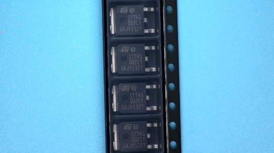
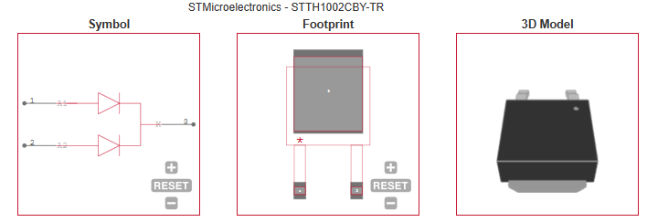
STTH1002CBY-TR STMicroelectronics DIODE ARRAY GP 200V 8A DPAK

label:
2024/06/6 274


CATALOG
STTH1002CBY-TR COUNTRY OF ORIGIN
STTH1002CBY-TR PARAMETRIC INFO
STTH1002CBY-TR PACKAGE INFO
STTH1002CBY-TR MANUFACTURING INFO
STTH1002CBY-TR PACKAGING INFO
STTH1002CBY-TR EACD MODELS


COUNTRY OF ORIGIN
China


PARAMETRIC INFO
Type Switching Diode
Configuration Dual Common Cathode
Peak Reverse Repetitive Voltage (V) 200
Maximum Continuous Forward Current (A) 16
Speed Ultra Fast Recovery Rectifier
Peak Forward Voltage (V) 1.25@10A
Peak Non-Repetitive Surge Current (A) 50
Peak Reverse Current (uA) 5
Peak Reverse Recovery Time (ns) 25
Operating Junction Temperature (°C) -40 to 175
Minimum Storage Temperature (°C) -65
Maximum Storage Temperature (°C) 175
Minimum Operating Temperature (°C) -40
Maximum Operating Temperature (°C) 175
Supplier Temperature Grade Automotive


PACKAGE INFO
Supplier Package DPAK
Pin Count 3
Lead Shape Gull-wing
PCB 2
Tab Tab
Pin Pitch (mm) 2.3(Max)
Package Length (mm) 6.6(Max)
Package Width (mm) 6.2(Max)
Package Height (mm) 2.4(Max)
Package Diameter (mm) N/R
Package Overall Length (mm) 6.6(Max)
Package Overall Width (mm) 10.1(Max)
Package Overall Height (mm) 2.63(Max)
Seated Plane Height (mm) 2.63(Max)
Mounting Surface Mount
Package Material Plastic
Package Description Deca Watt Package
Package Family Name TO-252
Jedec TO-252AA
Package Outline Link to Datasheet


MANUFACTURING INFO
MSL 1
Maximum Reflow Temperature (°C) 260
Reflow Solder Time (Sec) 30
Number of Reflow Cycle 3
Standard IPC-1752
Reflow Temp. Source Link to Datasheet
Maximum Wave Temperature (°C) N/R
Wave Solder Time (Sec) N/R
Lead Finish(Plating) Matte Sn annealed
Under Plating Material NiP
Terminal Base Material Cu Alloy
Shelf Life Period 2 Years


PACKAGING INFO
Packaging Suffix TR
Packaging Tape and Reel
Packaging Document Link to Datasheet


ECAD MODELS


Продукт RFQ