|
|
| CATALOG |
TPS75501KTTR Country of Origin
|
TPS75501KTTR Parametric Info
|
TPS75501KTTR Package Info
|
TPS75501KTTR Manufacturing Info
|
TPS75501KTTR Packaging Info
|
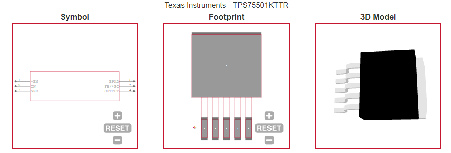
TPS75501KTTR ECAD Models
|
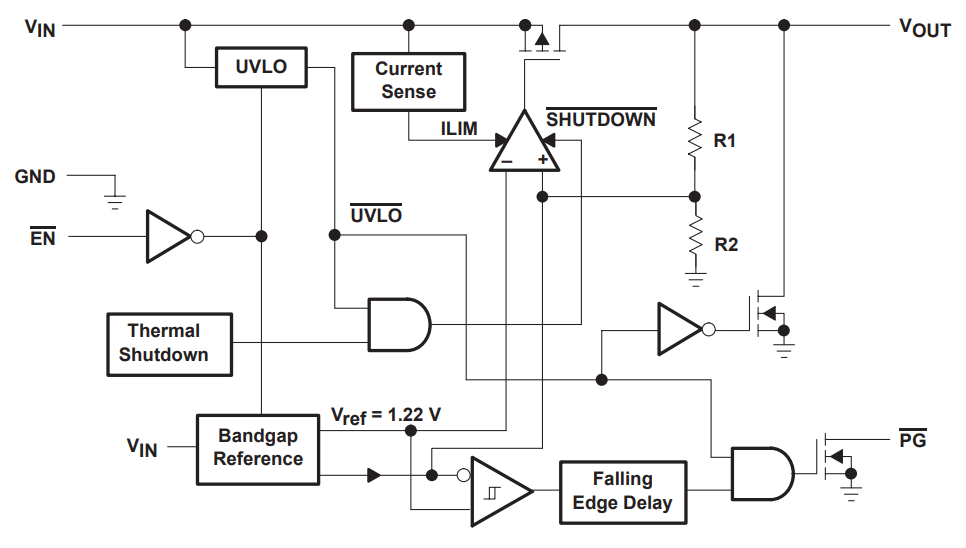
TPS75501KTTR functional block diagram
|
|
COUNTRY OF ORIGIN
|
China
|
Mexico
|
Malaysia
|
|
PARAMETRIC INFO
|
| Type |
LDO |
| Number of Outputs |
1 |
| Maximum Output Current (A) |
5 |
| Minimum Operating Temperature (°C) |
-40 |
| Maximum Operating Temperature (°C) |
125 |
| Output Type |
Adjustable |
| Output Voltage Range (V) |
<1.8|1.8 to 10 |
| Junction to Ambient |
38.7°C/W |
| Junction to Case |
2°C/W |
| Polarity |
Positive |
| Special Features |
Current Limit|Thermal Shutdown Protection |
| Load Regulation |
0.35%/V(Typ) |
| Line Regulation |
0.04%/V(Typ) |
| Maximum Quiescent Current (mA) |
0.2 |
| Maximum Dropout Voltage @ Current (V) |
0.5@5A |
| Minimum Input Voltage (V) |
2.8 |
| Maximum Input Voltage (V) |
5.5 |
| Output Voltage (V) |
1.22 to 5 |
| Typical Quiescent Current (mA) |
0.125 |
| Typical Dropout Voltage @ Current (V) |
0.25@5A |
| Reference Voltage (V) |
1.224(Typ) |
| Accuracy (%) |
±3 |
| Supplier Temperature Grade |
Extended |
|
|
PACKAGE INFO
|
| Supplier Package |
DDPAK |
| Basic Package Type |
Lead-Frame SMT |
| Pin Count |
6 |
| Lead Shape |
Gull-wing |
| PCB |
5 |
| Tab |
Tab |
| Pin Pitch (mm) |
1.7 |
| Package Length (mm) |
10.67(Max) |
| Package Width (mm) |
9.65(Max) |
| Package Height (mm) |
4.83(Max) |
| Package Diameter (mm) |
N/R |
| Seated Plane Height (mm) |
5.13(Max) |
| Mounting |
Surface Mount |
| Package Weight (g) |
N/A |
| Package Material |
Plastic |
| Package Description |
Double Deca Watt Package |
| Package Family Name |
TO-263 |
| Jedec |
TO-263BA |
| Package Outline |
Link to Datasheet |
|
|
MANUFACTURING INFO
|
| MSL |
2 |
| Maximum Reflow Temperature (°C) |
260 |
| Reflow Solder Time (Sec) |
N/A |
| Reflow Temp. Source |
Link to Datasheet |
| Maximum Wave Temperature (°C) |
N/R |
| Wave Solder Time (Sec) |
N/R |
| Lead Finish(Plating) |
Matte Sn |
| Under Plating Material |
N/A |
| Terminal Base Material |
Cu Alloy |
|
|
PACKAGING INFO
|
| Packaging |
Tape and Reel |
| Quantity Of Packaging |
500 |
| Packaging Document |
Link to Datasheet |
|
|
ECAD MODELS
|
|
|
FUNCTIONAL BLOCK DIAGRAM
|
|
|
|