|
|
• Feature options
– Split outputs (UCC53x0S)
– UVLO referenced to GND2 (UCC53x0E)
– Miller clamp option (UCC53x0M)
|
• 8-pin D (4mm creepage) andDWV (8.5mm creepage) package
|
• 60ns (typical) propagation delay
|
• 100kV/μs minimum CMTI
|
• Isolation barrier life > 40 Years
|
• 3V to 15V input supply voltage
|
• Up to 33V driver supply voltage
– 8V and 12V UVLO options
|
• Negative 5V handling capability on input pins
|
• Safety-related certifications:
– 7000VPK isolation DWV (planned) and 4242VPKisolation D per DIN V VDE V 0884-11:2017-01and DIN EN 61010-1
– 5000VRMS DWV and 3000VRMS Disolation rating for 1 minute per UL 1577
– CQC certification per GB4943.1-2011D and DWV (planned)
|
• CMOS inputs
|
• Operating temperature: –40°C to +125°C
|
|
| CATALOG |
UCC5320ECDR Parametric Info
|
UCC5320ECDR Package Info
|
UCC5320ECDR Manufacturing Info
|
UCC5320ECDR Packaging Info
|
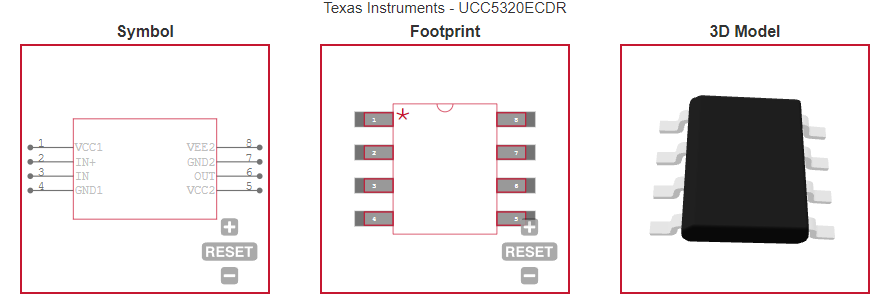
UCC5320ECDR ECAD Models
|
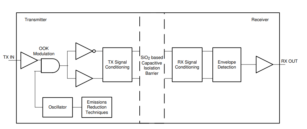
UCC5320ECDR Functional Block Diagram
|
UCC5320ECDR Applications
|
|
PARAMETRIC INFO
|
| Number of Drivers |
1 |
| Driver Configuration |
Inverting|Non-Inverting |
| Input Logic Compatibility |
CMOS |
| Maximum Operating Supply Voltage (V) |
15 |
| Peak Output Current (A) |
4.4(Typ) |
| Minimum Operating Temperature (°C) |
-40 |
| Type |
IGBT|GaNFET|MOSFET|SiCFET |
| Maximum Operating Temperature (°C) |
125 |
| Number of Outputs |
1 |
| Maximum Power Dissipation (mW) |
1140 |
| Minimum Operating Supply Voltage (V) |
3 |
| Maximum Supply Current (mA) |
73 |
| Absolute Propagation Delay Time (ns) |
75 |
| Maximum Propagation Delay Time (ns) |
72 |
| Maximum Rise Time (ns) |
28 |
| Maximum Fall Time (ns) |
25 |
| Latch-Up Proof |
No |
| Special Features |
Under Voltage Lockout |
| Minimum Storage Temperature (°C) |
-65 |
| Maximum Storage Temperature (°C) |
150 |
|
|
PACKAGE INFO
|
| Supplier Package |
SOIC |
| Basic Package Type |
Lead-Frame SMT |
| Pin Count |
8 |
| Lead Shape |
Gull-wing |
| PCB |
8 |
| Tab |
N/R |
| Pin Pitch (mm) |
1.27 |
| Package Length (mm) |
5(Max) |
| Package Width (mm) |
3.98(Max) |
| Package Height (mm) |
1.5(Max) |
| Package Diameter (mm) |
N/R |
| Package Overall Length (mm) |
5(Max) |
| Package Overall Width (mm) |
6.19(Max) |
| Package Overall Height (mm) |
1.75(Max) |
| Seated Plane Height (mm) |
1.75(Max) |
| Mounting |
Surface Mount |
| Package Weight (g) |
N/A |
| Package Material |
Plastic |
| Package Description |
Small Outline IC |
| Package Family Name |
SO |
| Jedec |
MS-012AA |
|
|
Manufacturing Info
|
| MSL |
2 |
| Maximum Reflow Temperature (°C) |
260 |
| Reflow Solder Time (Sec) |
30 |
| Number of Reflow Cycle |
3 |
| Standard |
J-STD-020D |
| Reflow Temp. Source |
Link to Datasheet |
| Maximum Wave Temperature (°C) |
N/R |
| Wave Solder Time (Sec) |
N/R |
| Lead Finish(Plating) |
Au |
| Under Plating Material |
Pd over Ni |
| Terminal Base Material |
Cu Alloy |
|
|
PACKAGING INFO
|
| Packaging Suffix |
R |
| Packaging |
Tape and Reel |
| Quantity Of Packaging |
2500 |
| Reel Diameter (in) |
13 |
| Reel Width (mm) |
12.4 |
| Tape Pitch (mm) |
8 |
| Tape Width (mm) |
12 |
| Component Orientation |
Q1 |
| Packaging Document |
Link to Datasheet |
|
|
ECAD MODELS
|
|
|
FUNCTIONAL BLOCK DIAGRAM
|
|
|
APPLICATIONS
|
• Motor drives
|
• High voltage DC-to-DC converters
|
• UPS and PSU
|
• HEV and EV power modules
|
• Solar inverters
|
|
|